Find what matters.
Search requires at least 3 characters
No result found
Quick links
Suggested searches
Search requires at least 3 characters
No result found
Quick links
Suggested searches


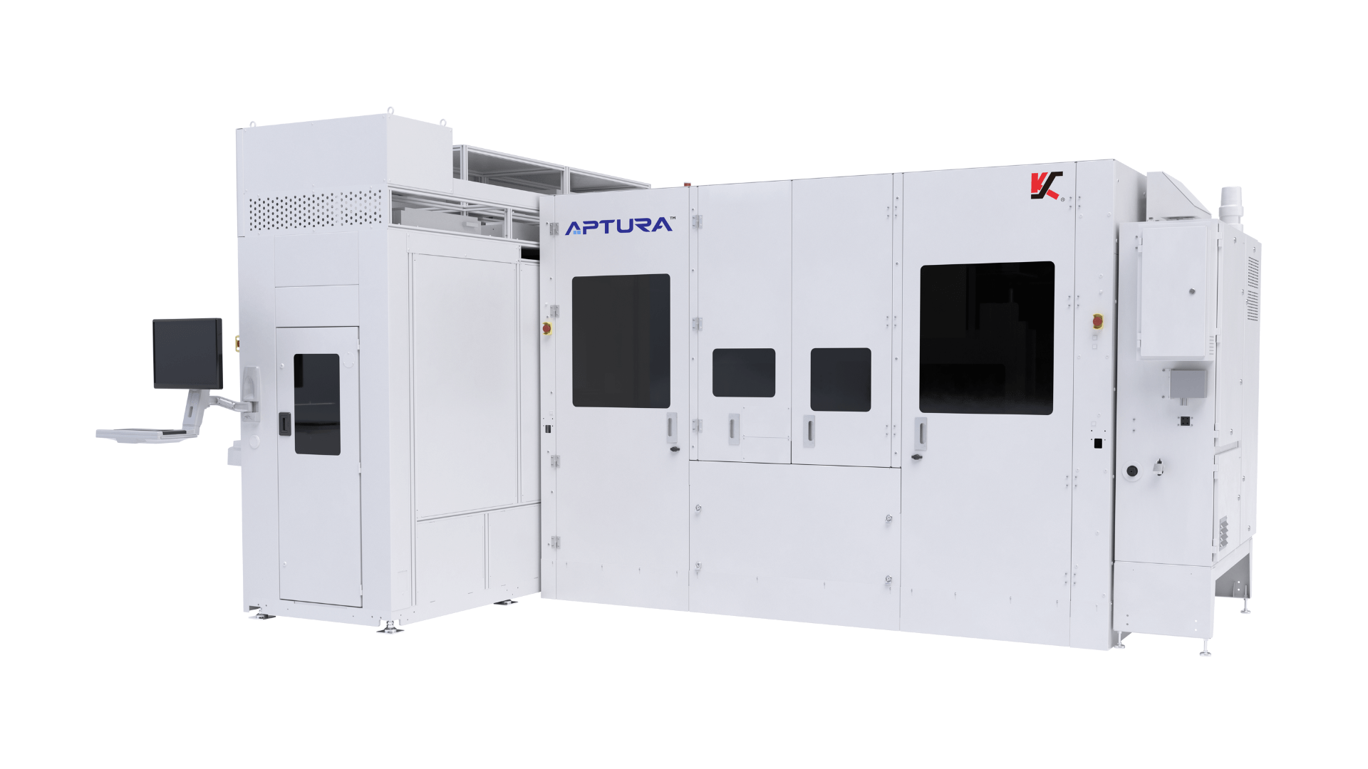
Industry-leading process monitors features to prevent yield loss during production.

Qualified in major OSATs for TC-CUF, TC-NCF, and TC-NCP processes.